

Battery Management Systems (BMS) are fundamental to ensuring the safety, stability and dependable operation of modern energy storage platforms. While system architecture and software algorithms are critical for functional control, safety performance is ultimately governed by hardware integrity. In real-world operating conditions, where electrical noise, thermal stress and high-energy transients coexist hardware design determines whether protection strategies operate as intended.
BMS with critical functional blocks including Microcontroller units (MCUs), clock circuits, MOSFETs, shunt and balancing resistors, DC-DC converters, analog front-ends (AFEs), ADCs, and sensing/measurement circuits. BMS designs must address unique challenges in material selection, stackup architecture, high-voltage isolation, current handling, signal integrity, and thermal dissipation.
Battery system safety is not the result of a single design decision. It emerges from the coordinated interaction of semiconductor packaging, power distribution networks, PCB layout practices, thermal management, grounding strategy and isolation design. From the smallest internal bond wire inside an integrated circuit to the full battery pack interface every physical implementation choice directly influences sensing accuracy, protection response time and long-term reliability.
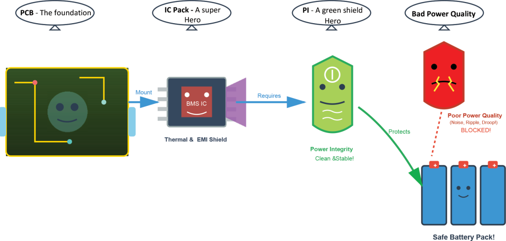
This article explores how IC packaging, power integrity and PCB layout collectively establish the foundation of BMS safety and why these elements must be engineered as a unified system rather than independent design tasks.
THE KEY INSIGHT
“Poor IC packaging creates parasitic elements (L, C, R) that corrupt power delivery. Without proper power integrity design (PDN, decoupling, grounding), the BMS IC receives noisy power inaccurate measurements BMS SAFETY FAILURE!
The Hardware Chain behind Battery Safety
A battery management system simultaneously performs multiple safety-critical functions:
- Voltage and current monitoring
- Temperature sensing
- Protection control
- Cell balancing
- Estimating SOC (State of Charge) and SOH (State of Health)
- Data communication and diagnostics
Each function depends on precise electrical measurements. Even small deviations caused by voltage ripple, overcharging, short circuit, physical damage, electromagnetic interference or thermal drift can propagate through the system and influence protection decisions. When measurement fidelity degrades, the entire safety framework becomes vulnerable.
Cell voltage routing in the PCB
Voltage tracks of each cell of the battery pack should have symmetrical track length, width and spacing while routing to the AFE chip to avoid RI(EMI/EMC) and to take care of the accurate measurement of cell voltages by AFE chip The BMS hardware to ensure that the battery charging current can be regulated based on the state of charge (SOC) and battery temperature.
Battery Management System (BMS) prevents it by monitoring temperature and disconnecting the battery during unsafe conditions. Reliable safety performance therefore depends on the stability of the entire hardware signal chain.
Why IC Packaging Matters More Than Expected
Integrated circuit packaging is often perceived as a mechanical enclosure. In reality, it significantly influences electrical, thermal and reliability behaviour at the system level.
Electrical Performance
Within an IC package, bonding wires and internal interconnects introduce parasitic resistance and inductance. These parasitic elements affect:
- Signal propagation characteristics
- Noise susceptibility
- Power distribution stability
- Measurement precision
In precision analog monitoring circuits, even micro-level disturbances originating at the package level can propagate through PCB traces and appear as sensing inaccuracies. Package selection therefore shapes system performance long before layout routing begins.
Thermal Effect
Thermal management is at the heart of reliable BMS operation. IC packages also determine how efficiently heat is transferred from semiconductor junctions to the surrounding environment. Inadequate thermal dissipation increases junction temperature, which may result in:
- Parameter drift in sensing circuits
- Reduced component lifespan
- Slower protection response
- Long-term reliability degradation
Effective thermal design requires alignment between package characteristics and PCB copper distribution, thermal vias and component placement strategy. Hot spots are identified and mitigated through design iteration. Additional calculated heat spreading structures are added as required to meet thermal specifications.
Thermal Management Strategies :
- Integrating fin-type heat exchangers on the outer casing or using a U-tube heat exchanger.
- Applying Phase Change Material (PCM) combined with an external coolant system.
- Using advanced solutions such as vapor chambers, cooling pipes, or thermoelectric coolers (higher cost).
- Adopting immersion cooling techniques, which effectively reduce operating temperature.
- MCUs, crystal oscillators, and precision references must be located in the coolest regions of the PCB.
Power Integrity: The Foundation of Stable Operation
While IC packaging defines intrinsic component behaviour, system-level safety depends on stable and predictable power delivery.
Power integrity refers to maintaining consistent voltage levels across all operating conditions. In BMS applications, unstable supply rails can introduce offset errors in measurement circuits or unpredictable behaviour in digital control logic.
Common sources of power instability include:
- Rapid load transients
- Switching converters
- Long current return paths
- Insufficient decoupling
Even minor ripple or ground bounce can shift analog reference levels, directly influencing protection thresholds.
Designing for Robust Power Delivery
Effective power integrity design requires:
- Placing decoupling capacitors close to IC supply pins
- Implementing low-impedance power and ground planes
- Minimizing loop inductance in high-current paths
- Separating noisy switching domains from sensitive analog supplies
Stable power delivery ensures that monitoring circuits operate within calibrated limits and maintain consistent protection accuracy.
PCB Layout: The Bridge between IC and System
Once component-level behaviour and power stability are addressed, PCB layout becomes the structural framework that integrates these elements into a functional system.
A BMS PCB must simultaneously satisfy two conflicting requirements:
- Safely conduct high currents
- Preserve microvolt-level measurement precision
Achieving this balance requires deliberate organization of board regions and careful routing strategy.
Functional Zoning
Dividing the PCB into functional zones improves performance and reduces interference:
- Power handling regions
- Analog sensing areas
- Digital processing blocks
- Communication interfaces
Physical separation limits electromagnetic coupling and prevents switching noise from contaminating sensitive measurement traces.
Grounding and Return Path Integrity
Ground strategy is one of the most critical contributors to measurement stability and overall safety.
A continuous ground plane provides predictable return paths and minimizes impedance variation. Fragmented or poorly managed ground structures create unintended loops and voltage offsets that directly distort sensing references.
Best practices include:
- Maintaining uninterrupted ground planes
- Avoiding trace routing across ground splits
- Using stitching vias to maintain continuity
- Controlling return current paths for analog signals
Proper grounding stabilizes reference voltages and strengthens protection reliability.
Managing Electromagnetic Interference across the Stack
BMS designs require a minimum of 4-layer stackups, with 6-layer or more complex structures recommended for high-performance applications. Electromagnetic interference (EMI) can originate from internal switching circuits or external electrical environments. If unmanaged, EMI couples into sensitive traces and propagates through package interconnects, compromising signal integrity.
Effective mitigation strategies include:
- Short and direct routing paths
- Differential signal routing where appropriate
- Guard traces around sensitive nodes
- Adequate spacing between power and analog circuitry
A continuous, uninterrupted ground plane is essential for effective EMI control. The stackup should minimize ground plane splits and cutouts, which can compromise electromagnetic compatibility. Reducing EMI preserves sensing accuracy and ensures protection mechanisms respond only to genuine fault conditions.
Isolation and High-Voltage Design Considerations
Battery systems often operate across multiple voltage domains. Proper isolation protects circuitry, users and connected systems.
Two parameters govern safe spacing:
- Creepage distance (surface path separation)
- Clearance distance (air gap separation)
Adequate spacing prevents dielectric breakdown caused by voltage surges, humidity or contamination. Isolation design must extend consistently from IC pins to PCB traces and connectors, ensuring uninterrupted protection throughout the system.
Standards Compliance : Design teams must adhere to international safety standards, including IEC & ISO Functional safety standards.
High-Current Path Design
High-current interconnects must be designed to minimize DC IR drop and power dissipation.
The design process follows a systematic approach:
- Initial Sizing: Trace widths are calculated per IPC specifications based on rated current and acceptable temperature rise
- Simulation Validation: DC resistance and power dissipation are verified through layout simulation to ensure performance remains within target budgets
- Thermal Analysis: Joule heating effects are evaluated using thermal simulation tools
- Design Optimization: Copper thickness, trace width, and supplementary structures are optimized to meet loss budgets
Advanced Current Handling Techniques – For applications requiring very high current capacity, designers employ:
- Increased Copper Weight: 2 oz or heavier copper layers
- Bus Bars: Solid copper bars or thick copper pours
- Reinforcement Connectors: Additional mechanical and electrical connections ensure robust current distribution
- Parallel Via Arrays: Multiple vias distribute current and reduce localized heating
Thermal Integrity from Package to PCB
Thermal management begins inside the semiconductor package and continues through PCB copper layers and mechanical structure.
Effective thermal design incorporates:
- Copper pours functioning as heat spreaders
- Thermal vias beneath power components
- Balanced heat source distribution
- Avoidance of localized thermal clustering
Thermal imbalance alters electrical characteristics and may degrade sensing precision, indirectly impacting protection decisions.
Protection Design and Transient Immunity
External interfaces expose BMS hardware to electrostatic discharge (ESD), surge events and fast transients. Protection components must intercept these disturbances before they reach sensitive ICs.
Effective placement requires:
- Locating protection devices near entry points
- Providing short, low-impedance discharge paths
- Ensuring robust grounding connections
Early transient suppression prevents high-energy events from propagating across the PCB and destabilizing internal circuitry.
Design Best Practices : Kelvin Sensing
All sensing paths must implement true Kelvin connections. Kelvin sense resistors should be placed symmetrically and as close as possible to the measurement point. Differential sensing configurations minimize common-mode errors and ground offset effects.
Validation: Closing the Safety Loop
Before deployment, hardware must be validated under realistic electrical, thermal and environmental conditions.
Critical verification steps include:
- Design rule verification
- Power integrity simulation
- Thermal analysis
- Signal integrity evaluation
- Environmental and stress testing
Validation confirms that IC packaging, power delivery, grounding and layout operate as a unified and stable system.
Conclusion
Battery management system safety is defined not solely by algorithms but by the physical integrity of the hardware stack. IC packaging governs intrinsic electrical and thermal behaviour. Power integrity ensures stable operating conditions. PCB layout integrates these elements into a coherent platform capable of maintaining measurement fidelity under stress.
When packaging characteristics, grounding strategy, isolation design and thermal management are optimized together, monitoring accuracy improves, protection mechanisms respond predictably and long-term reliability increases.
Designers who treat safety as a continuous engineering chain from semiconductor package to full pack implementation build energy systems capable of performing consistently in demanding real-world environments. Ultimately, successful BMS designs emerge when electrical, thermal and mechanical disciplines converge into a unified hardware strategy rather than operating as isolated domains.


